
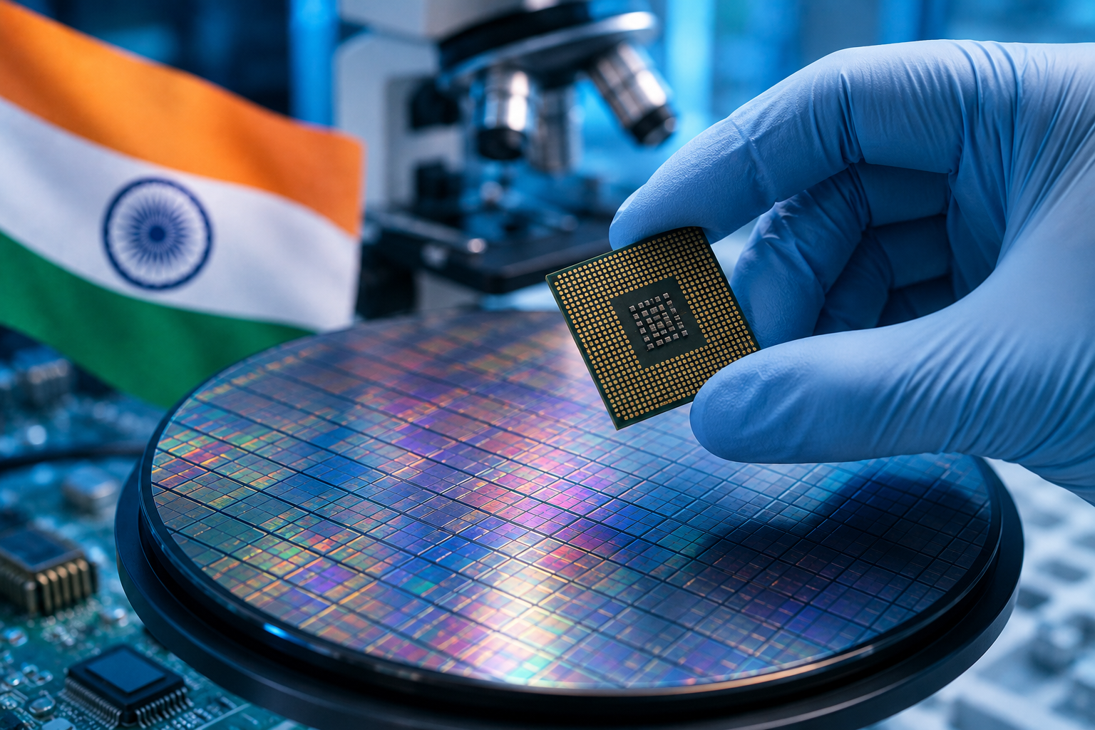
Sub-headline: Semicon 2.0 expands government support across chip design, fabrication, packaging, equipment, materials, R&D and talent. The semiconductor ecosystem is also expected to create 50,000–60,000 direct jobs.
Highlights:
- Government notifies all six pillars of Semicon 2.0
- Scheme covers design, fabs, ATMP/OSAT, R&D and talent
- Support extended to semiconductor machines and materials
- India targets development of another one lakh semiconductor engineers
- More than 250 chips designed by students from Tier-II and Tier-III cities
- Semiconductor ecosystem could generate 50,000–60,000 direct jobs
The Government has notified all six pillars of the Semicon 2.0 Scheme, significantly expanding policy support for India’s semiconductor ecosystem across chip design, manufacturing, packaging, equipment, materials, research and talent development.
Union Electronics and Information Technology Minister Ashwini Vaishnaw outlined the government’s vision for the next phase of India’s semiconductor programme during a media briefing on August 31, 2026.
Semicon 2.0 builds on the first Semicon India Programme and has six key pillars — design, machines and materials, additional fabrication units, strengthening the ATMP and OSAT industry, research and development, and talent development.
Under the design pillar, support will be available for semiconductor intellectual property, chips, System-on-Chips and modules catering to national and strategic priorities. Commercial-sector designs will also be covered, along with a Deployment-Linked Incentive for semiconductor IPs, chips and SoCs.
The machines and materials pillar aims to strengthen the domestic ecosystem required for semiconductor manufacturing.
Support for fabrication will cover silicon semiconductor wafer fabs as well as compound semiconductors, photonics, sensors including MEMS, discrete semiconductors and display fabs.
Another pillar will focus on expanding Semiconductor Assembly, Testing, Marking and Packaging (ATMP) and Outsourced Semiconductor Assembly and Test (OSAT) facilities. Dedicated support will also be provided for advanced R&D and workforce development.
Vaishnaw said India has developed 85,000 semiconductor engineers in four years, against an original target that was to be achieved over 10 years. The government has now set a target of developing another one lakh semiconductor engineers.
Students from Tier-II and Tier-III cities have also designed more than 250 chips, according to the minister.
India is expected to account for close to 10% of the global semiconductor industry’s market in the coming years. The domestic semiconductor ecosystem could also create around 50,000–60,000 direct jobs.
Projects supported under Semicon 2.0 will generally have a duration of up to six years, while applications under the scheme will initially remain open for three years.
The India Semiconductor Mission will act as the nodal implementation agency. It will invite applications, carry out technical and financial appraisals, recommend eligible applicants and monitor implementation.
A mid-term assessment is planned after three years of implementation, or earlier if required, to evaluate the programme’s impact and determine possible modifications or continuation.